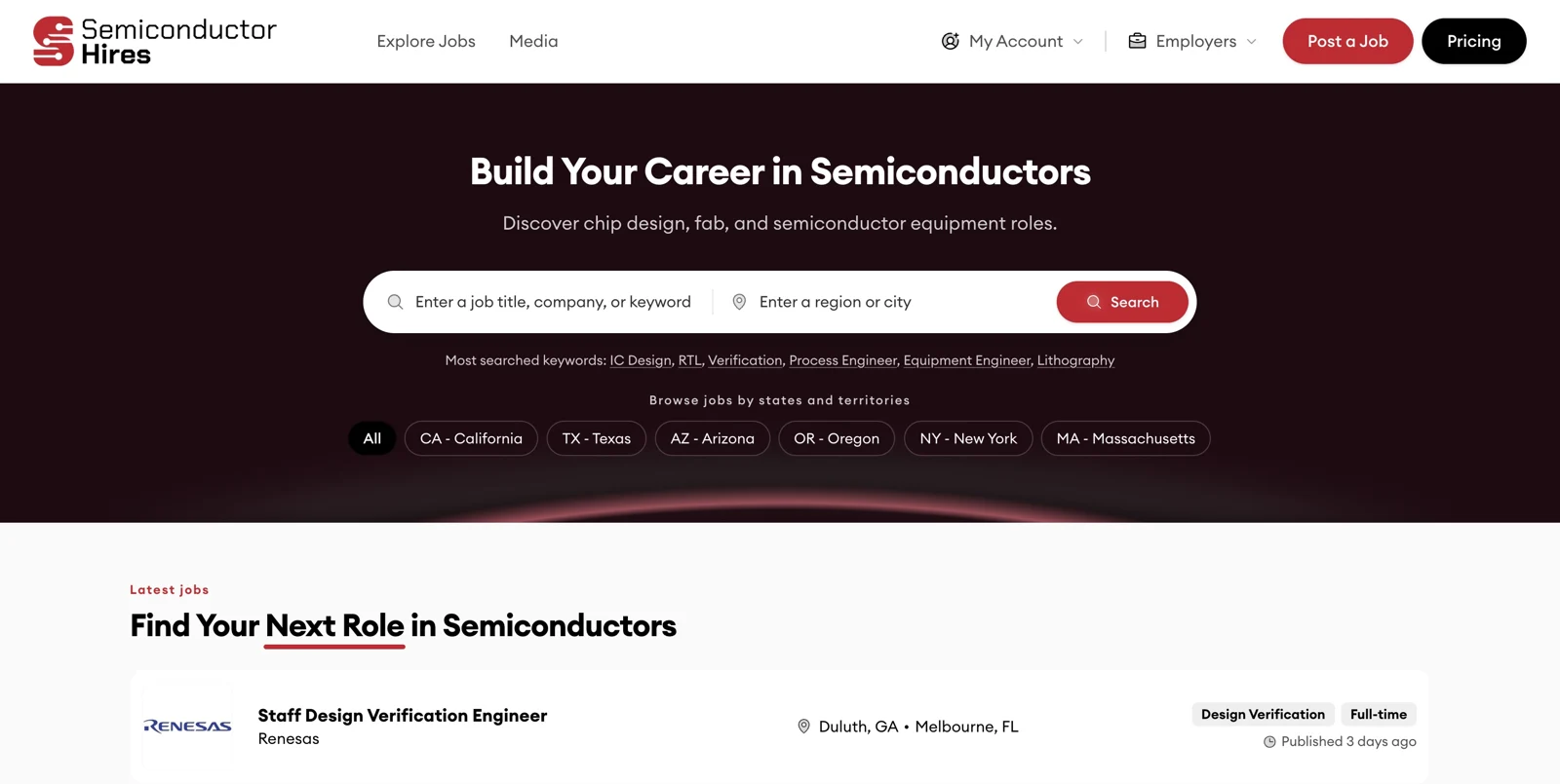
A chip moves through design, fabrication, testing and packaging before it becomes a usable component. SemiconductorHires follows those stages through semiconductor jobs in the United States. Its audience includes designers, process engineers, verification specialists and the professionals supporting semiconductor manufacturing equipment. Design verification, physical design and fabrication processes provide technical specialisms. Yield engineering, testing and packaging add later-stage responsibilities, while materials and applications roles fit when chips are central to the work. Chip designers and verification teams work on intended behaviour, fab engineers develop manufacturing processes and yield specialists analyse results, creating distinct engineering roles across the chain that turns an integrated circuit design into a packaged semiconductor product. Fab equipment expertise offers a route distinct from circuit design. The specific device, development stage and balance between engineering, production and support help explain what a semiconductor opening requires and where a candidate's experience will be useful.
SemiconductorHires provides automated job posting using more than 50 ATS connections, alongside individual advertisements and job packs. Chip industry employers can choose how to publish one specialist opening or several relevant design, fabrication, equipment and testing appointments held in recruitment software. Those routes serve appointments across the semiconductor product and production chain.